Introduction
Power Dissipation – the process in which electrical/electronics devices produce heat due to inefficiencies.
Power dissipation in CMOS?
Ultimate goal of VLSI engineers ?
Design and develop high performance, longer battery life, lower system costs, and less heat generation.
Power dissipation leads to – reduce time of operation, reduce mobility, increase operational cost, increase power consumption etc.
Low power design
In CMOS power dissipation – total energy consumed by static and dynamic components.

Static components : Refers to logic gates which output state remains unchanged as long as the input conditions are change. Eg. CMOS inverter
Dynamic Components : circuits that operates for temporay storage of logic states. Eg. Dynamic flip flop
Power Dissipation in CMOS

Static Power Dissipation
Power dissipated by the transistor when it is not switching i.e. when it is static.
i.e. when the input at the gate of the transistor is not transitioning either from 0 to 1 or from 1 to 0.
Static Power or leakage power
a) Subthreshold leakage b) Gate Leakage c) Junction Leakage
Subthreshold leakage

We know Nmos= ON when Vgs > Vth,
When Vgs <Vth, Nmos = Off;
In real Transistor, current falls down exponentially and small current flows from drain to source.
Sub threshold current is the current which flows between drain and source when Vgs < Vth (for nmos) or Vsg < |Vth| (for pmos)
b) Gate Leakage
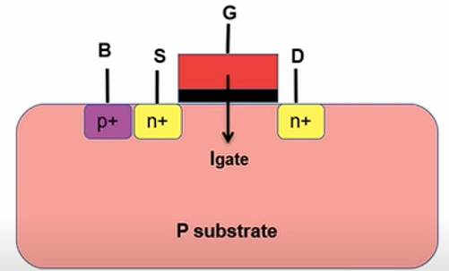
When gate oxide is very thin, then it allows current to pass through it
c) Junction Leakage
PN junction in a CMOS formed diodes, these diodes are in reversed bias. But reverse bias still conducts small amount of current, this cause junction leakage current
Dynamic Power Dissipation
Dynamic power dissipation– power dissipated when circuit is active.
Classifications :
a) Switching Power Dissipation b) Internal Power Dissipation
Switching Power : power dissipated while charging & discharging the load capacitor at the output of the cell.

fig (a) When input switches from 1 to 0 fig (b) When input switches from 0 to 1
Internal Power : any power which is dissipated within the boundary of a cell.
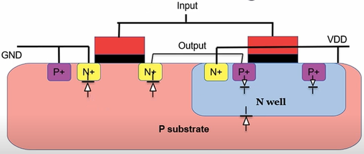
i) Short Circuit Power
ii) Power needed to charge /discharge the internal nodes of a transistor
Short circuit Power : power dissipated when both pmos & nmos are on simultaneously during input transition

Pmos is on when : Vss <= Vi <= Vdd –Vt
Nmos is on when : Vt < =Vi <=Vdd
Then both pmos and nmos are on for : Vt<=Vi<= Vdd - Vt
How to overcome/Reduce/Minimize from Power Dissipation in CMOS
Control supply voltage :Reducing the supply voltage requirement (Vdd).
Reduce dynamic power : Dynamic power is the power consumed when the circuit is in operation.
Done by Reducing the clock frequency, supply voltages, or dynamic effective capacitance
Power optimization techniques: using power optimization techniques like clock gating, power gating, and voltage scaling to reduce power consumption.
For example, in clock gating, we can add more logic gates to the circuits to trim the clock tree.